IC foundries overview (final part)
A detailed overview on the IC foundry industry with the main players. In this part: VIS (Vanguard International Semiconductor), Dongbu HiTek (DB-HiTek) and Powerchip (PSMC).
VIS (Vanguard International Semiconductor)
VIS (Vanguard International Semiconductor), headquartered in Taiwan is a semiconductor foundry known for MEMS fabrication, power management solutions, high-efficiency optical sensors, and voltage-optimized technologies designed for consumer electronics and computing displays. This diverse portfolio underscores the company's ability to address multifaceted market needs through its tailored and cutting-edge semiconductor solutions.
At the core of VIS's success lies a steadfast dedication to staying at the forefront of technological advancements across a wide spectrum of semiconductor processes, spanning from 1um and 0.18um and beyond. This commitment enables the company to consistently pioneer innovative solutions that meet the evolving demands of various industries.
As a top-tier IC pure-play foundry, VIS has strategically positioned itself in the semiconductor landscape. Key milestones in the company's growth trajectory include the acquisition of fab5 from Winbond in 2008, fab3 from Nanya Technologies in 2014 and the purchase of Globalfoundries' 8-inch fab in Singapore in 2019. These strategic moves have propelled VIS's capabilities, leveraging advanced process technologies and establishing a robust presence in MEMS fabrication.
Notably, VIS's industry credibility is further solidified by its association with TSMC, with the latter holding approximately 28% of VIS shares. This partnership not only underscores VIS's stature within the industry but also signifies strong industry backing and stability, bolstering the company's standing in the competitive semiconductor market.
Process Node Portfolio
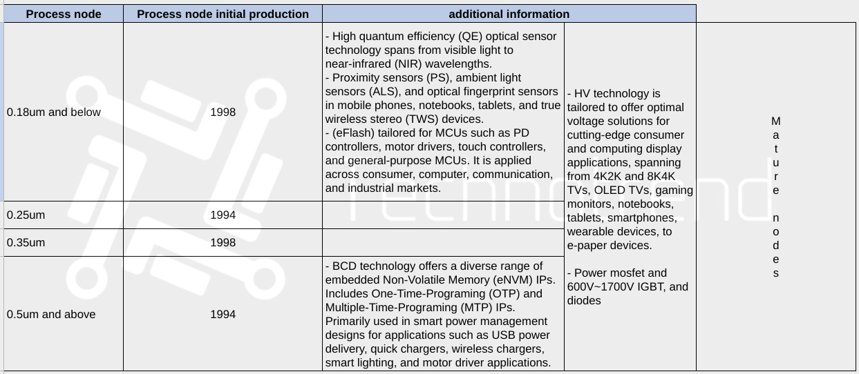
- 0.18um and advanced process technology account for 53% of total wafer revenue, demonstrating VIS's expertise in cutting-edge fabrication.
- 0.25um, 0.35um, and 0.5um nodes contribute 10%, 16%, and 21% of total wafer revenue, respectively, showcasing a diversified technological offering.
Key Applications by process nodes:
0.18um and Below:
- High QE optical sensor technology catering to various applications from visible light to NIR wavelengths.
- Targeted solutions for proximity sensors, ambient light sensors, optical fingerprint sensors used in mobile devices, notebooks, tablets, and TWS devices.
- Specialized (eFlash) for MCUs, finding applications across consumer, computer, communication, and industrial markets.
Across 1um and Up to 0.18um:
- HV technology designed for cutting-edge consumer and computing display applications, including TVs, OLED displays, gaming monitors, mobile devices, and e-paper technology.
- Expertise in Power mosfets, 600V~1700V IGBTs, and diodes.
0.5um and Above:
- BCD technology featuring embedded eNVM IPs, including OTP and MTP IPs, primarily utilized in smart power management designs for USB power delivery, quick chargers, wireless chargers, smart lighting, and motor driver applications.
VIS fab list
VIS operates with several manufacturing facilities, each contributing distinct capabilities to the company's technological prowess. Fab1, Fab2, Fab3, Fab5 located in Taiwan (Hsinchu and Taoyuan). Fab VS1, established in 2014 in Singapore, Moreover, VIS is contemplating the establishment of a new 12-inch fab in Singapore, earmarked for automotive chip production, further expanding its capabilities in specialized sectors.
VIS's strategic focus extends beyond conventional semiconductor production. Emphasizing MEMS, discrete components, and other specialized manufacturing areas, VIS demonstrates a commitment to pioneering technological advancements in niche segments within the semiconductor industry.
2023 Q3 financial snapshot
In the 2023 Q3 VIS quarter results, Power Management emerged as the dominant platform, constituting a substantial 63% share of the total wafer revenue. Meanwhile, the revenue distribution from other platforms showcased significant contributions as well, with LDDIC accounting for 24%, SDDIC for 9%, and Other platforms comprising 4% of the total wafer revenue. This distribution signifies the robust performance of VIS across various semiconductor platforms, highlighting the strength and diversity of its product offerings in the market.
An insightful glimpse into VIS's revenue distribution underscores the critical role played by their diversified technological offerings. The 2023 Q3 revenue reports a dominant performance in cutting-edge fabrication. Notably, 0.18um and advanced processes emerged as stalwarts, commanding a significant 53% of the total wafer revenue.
This robust performance finds complements in various nodes, each contributing to VIS's versatile technological spectrum. Nodes spanning 0.25um, 0.35um, and 0.5um secured respective shares of 10%, 16%, and 21% in the revenue distribution. Such diversified revenue allocation underscores VIS's adaptability across a myriad of applications, showcasing their proficiency in areas such as high QE optical sensors, proximity sensors, MCUs, advanced HV technology for consumer electronics, and BCD technology for smart power management.
Dongbu HiTek (DB HiTek)
Formerly Dongbu Group, DB started wafer production in 1983. Achieved 'high-purity poly-crystalline silicon' milestone in 1992. Ventured into semiconductor manufacturing in 1997, evolved into DB HiTek.
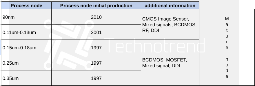
Dongbu Hitek, evolving from 0.35um to 90nm nodes, covering several applications, such as: CMOS Image Sensor, RF and DDI. Recently, DB-HiTek has started to supply Samsung Display's smartphone OLED DDI, presenting 40nm-based products in late 2023, thanks to a partnership with UMC, focusing on mid-to-low-end segments smartphones.
DB HiTek fab list
Dongbu Hitek's fabrication capabilities have expanded significantly over the years. Fab1, operational since 1997 in Bucheon, South Korea, specializes in nodes ranging from 0.15um to 0.18um and 0.25um to 0.35um, boasting an 8-inch wafer size. Looking ahead, plans are underway for a new fab, covering a new 12-inch wafer production between 2025 and 2030, with a capacity of 20,000 wafers per month.
Additionally, Fab2, established in 2001 in Sangwoo, South Korea, operates with nodes spanning from 0.13um/0.11um to 90nm, utilizing an 8-inch wafer size. These facilities represent Dongbu Hitek's commitment to technological advancement and readiness to embrace larger-scale production capabilities in the semiconductor industry.
Powerchip Semiconductor Manufacturing Corporation (PSMC)
Powerchip Semiconductor Manufacturing Corporation (PSMC) has established itself as a pioneering force in the semiconductor industry since its inception in 1994. Over the years, the company has garnered recognition for its specialization in dynamic memory manufacturing and wafer foundry services, showcasing an extensive range of expertise across various memory technologies like Flash NOR, NAND Flash, and DRAM.
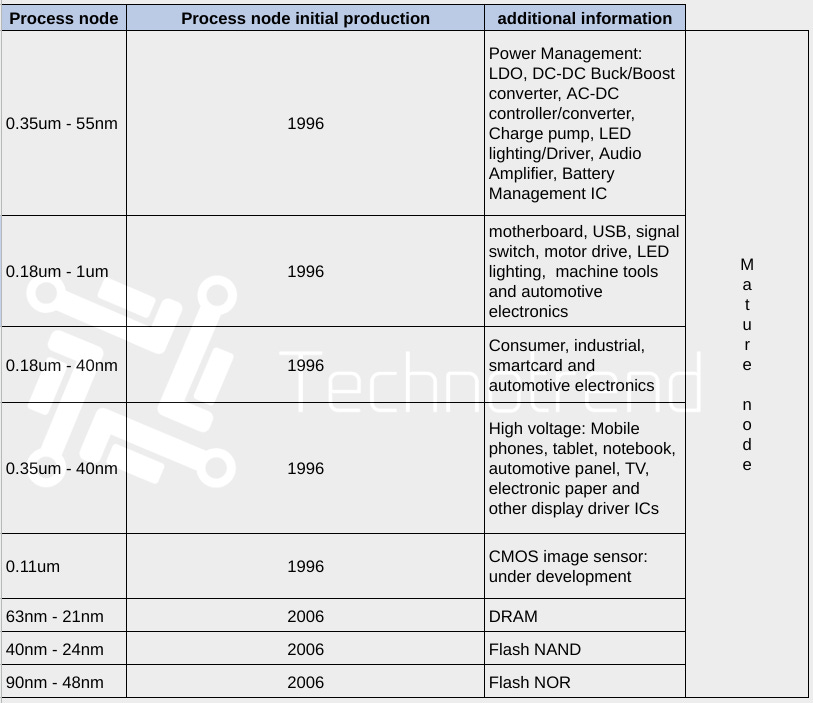
The diverse portfolio of PSMC's offerings extends across a broad spectrum of applications, spanning multiple industries and demonstrating the company's significant impact. From power management solutions encompassing LDO, DC-DC Buck/Boost converters, AC-DC controllers/converter, charge pumps, LED lighting/Drivers, audio Amplifiers, to manufacturing components for motherboards, USB interfaces, signal switches, motor drives, LED lighting, machine tools, and automotive electronics.
PSMC’s process node portfolio ranges from 0.35um to 21nm, each node serving distinct and crucial applications. From High Voltage applications addressing mobile phones, tablets, notebooks, automotive panels, TVs, electronic paper, and display driver ICs to innovative strides in CMOS image sensor development, the company consistently demonstrates its commitment to advancing cutting-edge technology.
In recent years, PSMC has focused into significant productions, stepping into DRAM manufacturing within the 63nm - 21nm range, contributing substantially to high-performance memory solutions. Additionally, its focus into Flash NAND technology from 40nm - 24nm signifies a pivotal contribution to high-density storage solutions, while its expertise in Flash NOR production from 90nm - 48nm underscores its provision of non-volatile memory solutions.
PSMC fab list
PSMC has established various manufacturing facilities in Taiwan, including the initial 8-inch wafer fab (Fab 8A) operating since 1985, alongside Fab 8B, which began in 1996, both specializing in DRAM production. Additionally, the company operates three 12-inch wafer fabs (P1/2, P3, and P5 Fabs) with a combined monthly capacity of about 130,000 wafers. This significant infrastructure makes PSMC the largest memory manufacturer in Taiwan.
In 2023, PSMC unveiled a major expansion plan in Miyagi prefecture, Japan, through a partnership with SBI Holdings. This development involves the construction of a new fab, with its initial production phase scheduled to commence in 2027. Initially focused on 40nm and 55nm technology, this phase aims to produce about 10,000 wafers monthly.


